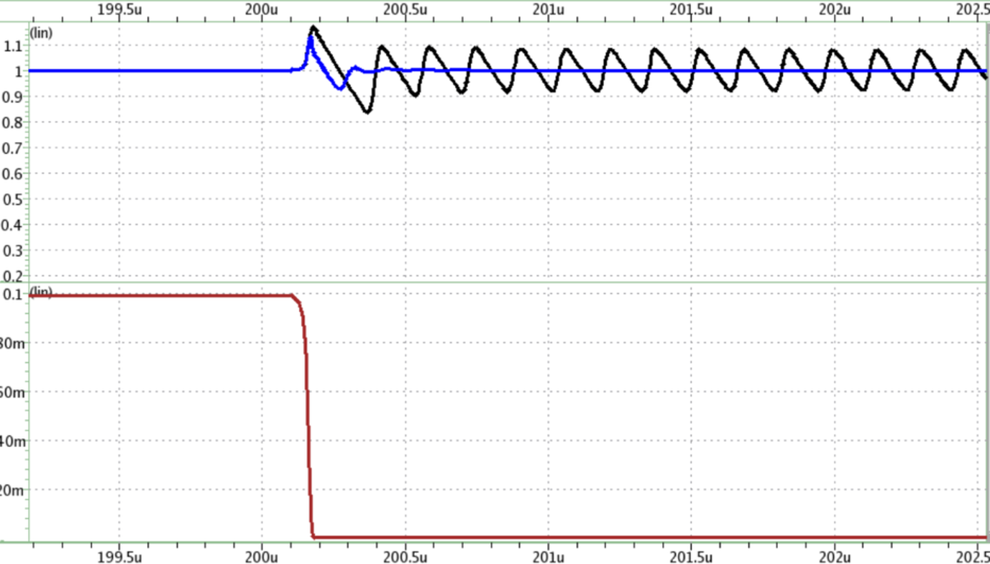
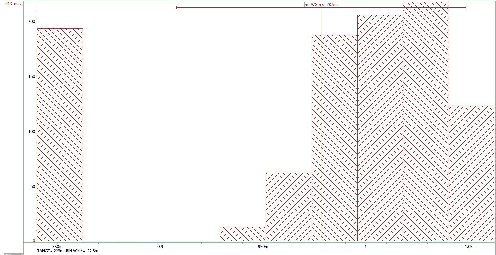
This project was based on a literature-proposed DFC architecture. I implemented and evaluated the circuit, performed small-signal and PVT/Monte Carlo verification, and added and iterated the transient-accelerator path.
Operating conditions
810
Monte Carlo samples
1000
Verification stage and scope
Schematic-level design and simulation study
Next focusThe next iteration will focus on heavy-load stability margin and reducing the transient accelerator’s non-ideal steady-state current.
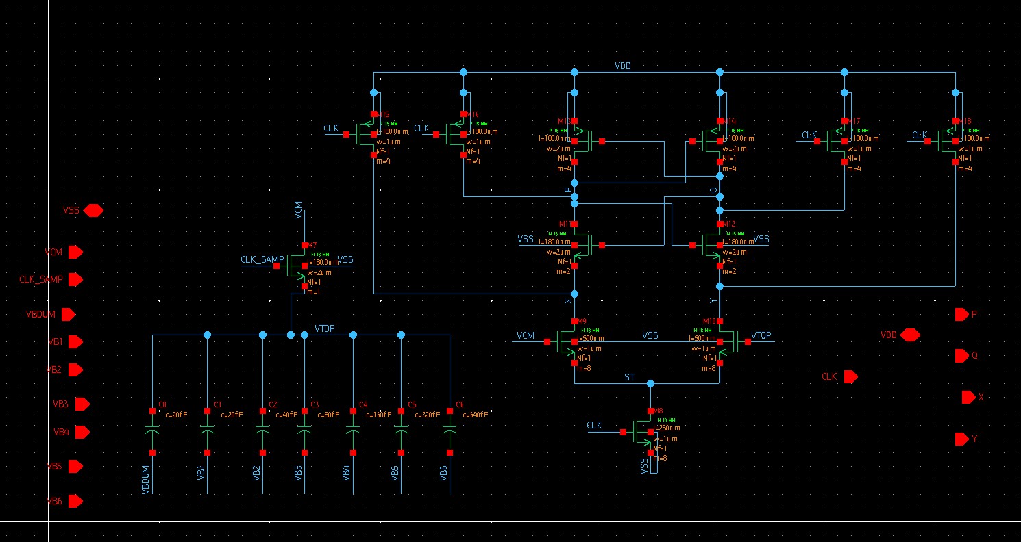
Completed the CDAC, StrongARM comparator, and floating-VTOP analog-front-end integration for a 6-bit SAR ADC, with design iterations that reduced kickback.
Resolution
6 bit
Nominal conversion error
−0.0469 LSB
Date
2026-07
Verification stage and scope
Transistor-level
Next focusThis phase completed the CDAC–StrongARM analog-front-end integration. Closed-loop control, linearity characterization, and physical verification are planned for the next stage.
Completed the schematic and pre-layout design of a 2.4 GHz inductively degenerated cascode common-source LNA in 180 nm CMOS. Across the 45-case PVT sweep, S12, noise figure, and input P1dB met their project targets in all cases, while output matching and bias/power robustness were identified as the main directions for the next design iteration.
PVT validation
45 cases
Core RF metrics
S12 / NF / P1dB
45/45
Date
2026
Verification stage and scope
Schematic
Next focusCo-optimization of output matching and bias/power robustness.
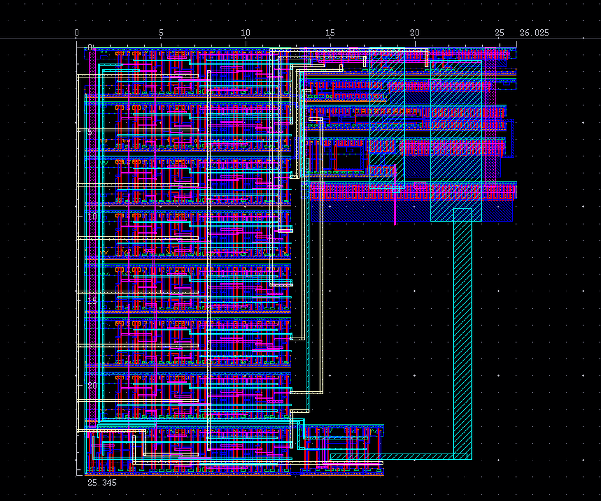
Completed a DLDO integrating a latch comparator, an 8-bit saturating UP/DOWN counter, a binary-sized PMOS array, and feedback, with pre- and post-layout behavior compared.
Verification level
Pre / Post
Physical-design result
Layout
completed for the reported circuit blocks
Verification stage and scope
Pre-layout and extracted post-layout simulation
Validation boundaryThe current results focus on relative pre- and post-layout behavior. Complete test conditions and signoff scope are required before making absolute specification comparisons.
Next focusComplete the test-condition documentation and further evaluate parasitic delay, clock skew, and layout asymmetry.